37 gallium indium phase diagram
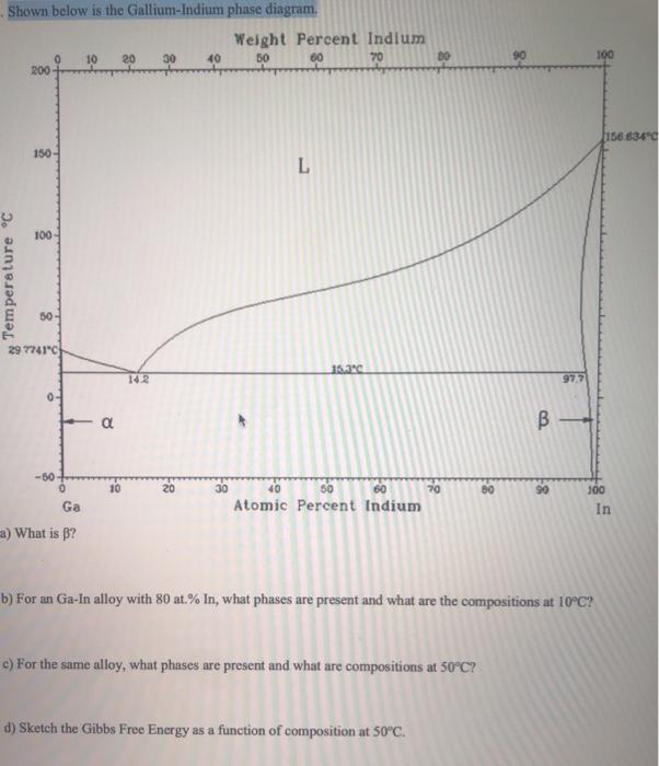
Nov 15, 2012 — This point is the eutectic temperature and composition. Based on the indium-gallium phase diagram, which depicts which phases are stable over a ...
However, indium is the major element in the catalyst. The relative ratio between In and Au is the same for both InP and GaP nanowires. Based on the HRTEM analysis in Fig. 4e, the catalyst phase is mainly of AuIn 2. The introduction of Ga does not reduce the In content but only leads to a small concentration of Ga in the catalyst.
Intrinsically stretchable conductors—such as room temperature liquid metals (eutectic gallium-indium, eGaIn 14), ionic conductors 15 and conducting polymers 16,17 —do not require sophisticated ...

Gallium indium phase diagram
The construction of a Light Emitting Diode is very different from that of a normal signal diode. The PN junction of an LED is surrounded by a transparent, hard plastic epoxy resin hemispherical shaped shell or body which protects the LED from both vibration and shock. Surprisingly, an LED junction does not actually emit that much light so the ...
The phase diagram, molecular dynamics, and mathematical modeling are used to predict, and the suitable extensible liquid metal polymer composites are selected through experiments. 2.3. The Application of Liquid Metal Composites in Scalable Circuits ... Gallium Indium alloy was used as ink material (melting point 52 °C). A desktop 3D printer ...
The present gallium-doped lead-free solder can also be applied to general soldering use with Ag materials. ... The other solders with low joint resistivity are indium film and lead-free Sn-Ag-Cu (SAC) solders ... which is the only stable alloy in the binary phase diagram at low temperature.
Gallium indium phase diagram.
Indium atoms have 49 electrons and the shell structure is 2.8.18.18.3. Diagram of the nuclear composition, electron configuration, chemical data, and valence orbitals of an atom of indium-115 (atomic number: - 2ACT1GN from Alamy's library of millions of high resolution stock photos, illustrations and vectors.
News: LEDs 16 September 2021. Increased current for red InGaN μLEDs. King Abdullah University of Science and Technology (KAUST) in Saudi Arabia has reported indium gallium nitride (InGaN) red micro-sized light-emitting diodes (μLEDs) aimed at meeting the color and power requirements of LED-based displays [Zhe Zhuang et al, Photonics Research, v9, p1796, 2021].
Gallium indium alloy (EGaIn 75.5% gallium and 24.5% indium) is a eutectic alloy with good fluidity and high conductivity at room temperature (the conductivity and viscosity of EGaIn are 3.4×10 4 s·cm-1 and 1.99×10⁻³ MPa/S) , .
According to the Ga-In phase diagram [ 7 ], the eutectic has the composition Ga-14.2 mol % In, and the eutectic temperature is Te = 288.3 K. In the hypereutectic region, an indium-based β solid solution forms with the solubility of gallium in indium of 2.2 mol %.
The goals of this work are as follows: (а) searching for a method of study of the In - Se system taking into account the specified problems and difficulties, (b) choosing a way for the instrumental implementation of this method, and (c) obtaining experimental evidence that this method and its implementation are promising. The choice of the In - Se system is related to the fact that indium ...
Gallium (Ga)-based liquid metals not only have excellent electrical and thermal conductivities with low viscosity and no toxicity [1,2], but are also environmentally friendly "green" materials because they can be recovered and recycled after use [].Among the Ga-based liquid metals, Ga-In eutectic alloy (EGaIn) is one of the most investigated liquid metals because it has a melting point ...
The GaN crystalline nanomesas have no threading dislocations, and do not show any V-pit. The effects of ambient gas and substrate symmetry on the growth of indium oxide thin films were studied. Un diagramme de phase precis dans la region riche en indium du systeme ternaire Ga-In-Sb a ete etabli. IV France Current journals.
by DM Zakharov · 1975 · Cited by 8 — On the base of thermodynamic analysis of the gallium-indium alloy system its eutectic concentration has been determined: 13.8+-0.4 at.
GaN microrods were grown on graphene-coated SiO2/Si substrates by metal-organic vapor phase epitaxy. ... well nanodisks 21, and indium gallium arsenide ... diagram of the procedure for ...
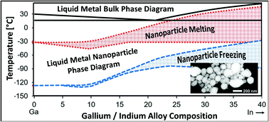
In. According to the phase diagram of the bulk gallium-indium alloy [ 8] the frozen alloy segregates into two phases: an In-rich solid solution with a structure of bulk crystalline indium and a phase with a structure of stable α-Ga, which has very low amount of dissolved indium.
Heterojunction AlGaAs / GaAs PIN Epitaxial Wafer. A 3-inch GaAs epitaxial wafer can be provided for making a PIN diode chip, which can make a power electronic device with high isolation and low insertion loss. A heterojunction AlGaAs/GaAs PIN wafer makes the diode with low RF on-state resistance suitable for fabricating various broadband switches.
They are blown dry with nitrogen and surface-oxidized in an oxygen plasma cleaner (Femto Diener) for approximately 8 min with a 10 sccm gas flow (10 Pa oxygen pressure). This surface treatment renders the wafers hydrophilic. For an experiment, liquid gallium-indium alloy is employed for bonding the wafer to a home-made copper stub.
Phase diagram of the cu-in system in this work. | download ...
Gallium is a chemical element with the symbol Ga and atomic number 31. Discovered by French chemist Paul-Émile Lecoq de Boisbaudran in 1875, Gallium is in group 13 of the periodic table and is similar to the other metals of the group (aluminium, indium, and thallium).. Elemental gallium is a soft, silvery metal at standard temperature and pressure.In its liquid state, it becomes silvery white.
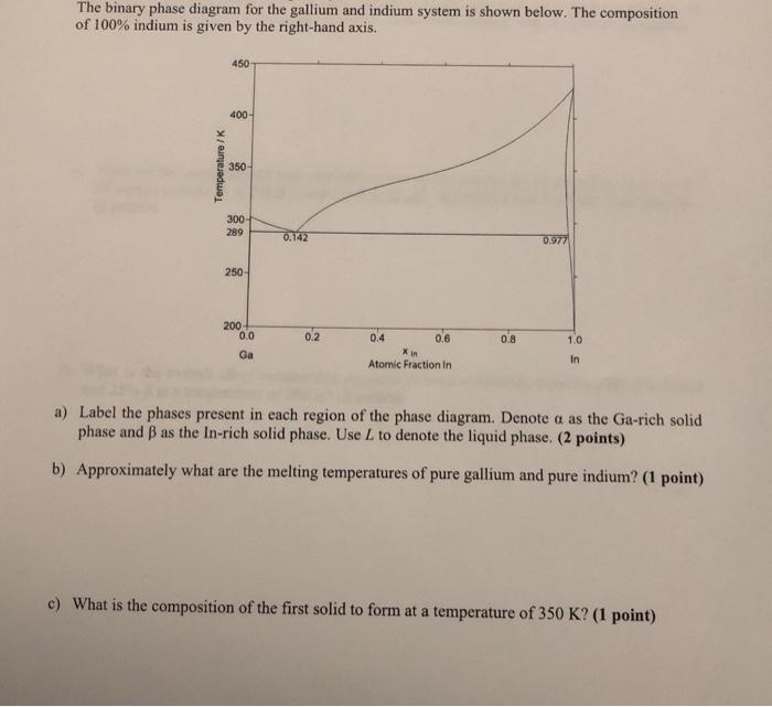
Solved the binary phase diagram for the gallium and indium | chegg.com
The phase diagram, molecular dynamics, and mathematical modeling are used to predict, and the suitable extensible liquid metal polymer composites are selected through experiments. 2.3. The Application of Liquid Metal Composites in Scalable Circuits ... Schematic diagram of formation of hydrated manganese dioxide on the surface of gallium indium ...
![Phase diagram of eutectic gallium-indium [5]. | Download ...](https://www.researchgate.net/publication/323553754/figure/fig5/AS:600806441099268@1520254826291/a-superconducting-transition-temperature-for-eGainsn-bulk-materials-and-nanoparticles_Q320.jpg)
Phase diagram of eutectic gallium-indium [5]. | download ...
by CJ Adams · 1950 — constructing the gallium-indium equilibrium diagram, . to investig te the alloys of gallium and.indium, and to recover the pure metals from their alloys.51 pages
Construction of gallium–tin nonequilibrium state diagram and its ...
by X Yin · 2011 · Cited by 6 — The eutectic temperature of Ga-In is 288.5K, below which temperature all gallium and indium is solid in the equilibrium state. Thus, the equilibrium state ...
![Phase diagram of eutectic gallium-indium [5]. | Download ...](https://www.researchgate.net/publication/323553754/figure/fig1/AS:600806436896776@1520254825769/Phase-diagram-of-eutectic-gallium-indium-5_Q640.jpg)
Phase diagram of eutectic gallium-indium [5]. | download ...
by TJ Anderson · 1991 · Cited by 132 — The Ga-In system is a simple eutectic type, with negligible solu- bility of In in solid (r. The assessed Ga-In equilibrium phase diagram (Fig.
Experimental investigations of phase equilibria in ternary ag-cu ...
The phase diagram, molecular dynamics, and mathematical modeling are used to predict, and the suitable extensible liquid metal polymer composites are selected through experiments. ... Schematic diagram of formation of hydrated manganese dioxide on the surface of gallium indium alloy liquid metal; (E) Schematic diagram of electrocatalytic ...
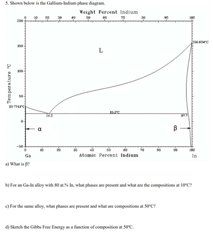
Solved 5. shown below is the gallium-indium phase diagram. | chegg.com
by AN Campbell · 1962 · Cited by 16 — It is possible that two peritectics exist at the latter temperature, in close proximity. The ternarl- eutectic lies at 14.j0 C and has an approximate con~ ...
Thermal properties of gallium indium arsenide antimonide (gainassb)
We studied two different junction materials: indium sulfide and gallium oxide. Indium sulfide (In 2 S 3) is an n-type semiconductor with an optical bandgap of 2.1-2.3 eV. It is considered an effective and nontoxic substitute for CdS and has been applied as a junction layer on CIGS-based solar cells.

Liquid gallium and the eutectic gallium indium (egain) alloy ...
The main phase of the leaching residue is In 2 O 3, and some mixed oxides of copper, indium and gallium. When the acid concentration exceeds 4 mol/L, the leaching reaction is basically completed, and the remaining residue includes incomplete volatile selenium and a small amount of indium oxide.
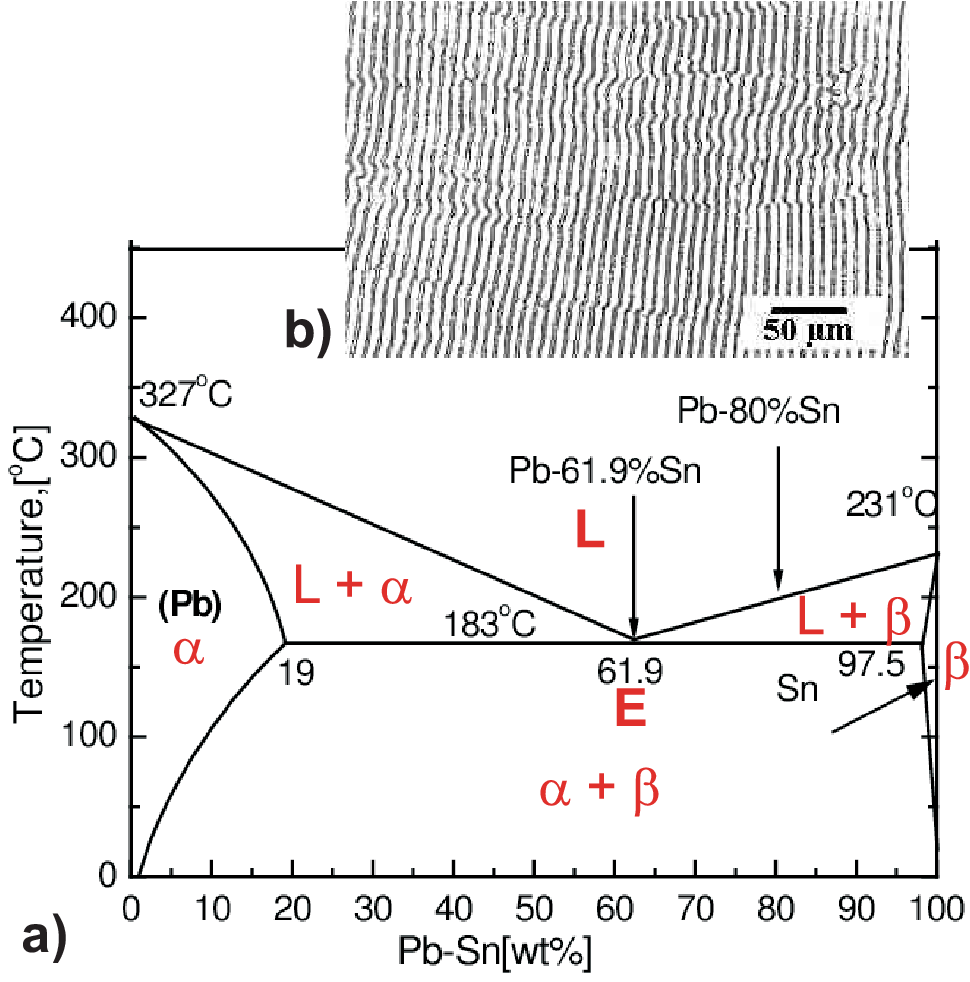
Eutectic phase diagrams
Initially, GaAs bandgap is 1. 43ev which is almost perfect for solar cells (solar panel diagram). Second, due to the fact that Gallium is a spin-off of the smelting of other metals, GaAs cells are fairly insensitive to heat and it can keep high performance when temperature is rather high. Third, GaAs has the broad range of design alternatives.
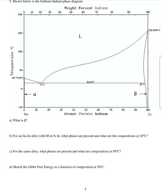
Solved 5. shown below is the gallium-indium phase diagram. | chegg.com
The indium 111- tagged white blood cell (WBC) scan is a type of imaging modality used to help identify regions of inflammation and thus infections when other imaging studies are equivocal or contraindicated.[1] Clinicians commonly use this test for diagnostic purposes in the evaluation of prosthetic joint infections, osteomyelitis, vascular graft infections, and fever of unknown origin.[1]

Melting curves of gallium, indium, thallium, and aluminum (it can ...
Gallium-based liquid metals, such as the eutectic gallium-indium (EGaIn) being an electrically conductive liquid phase at room temperature, have attracted immense interests as a promising candidate for deformable ... Based on the phase diagram of the Ga-In, 21.4 weight percentage (wt%) of In in the alloy ...

Us20050142685a1 - hermetic wafer-level packaging for mems devices ...
Herein, an electrochemical-inert liquid gallium-indium alloy coating is designed toward the zinc anode, inspired by the gallium-indium-zinc phase diagram. This unique liquid coating prefers an inward-deposition of Zn underneath the liquid coating assisted by ultrafast mass/charge transport when charging.
Solved 5. shown below is the gallium-indium phase diagram. | chegg.com
Download scientific diagram | Phase diagram of eutectic gallium-indium [5]. from publication: Recent progress on liquid metals and their applications ...
Sciencemadness discussion board - gallium-aluminium alloy ...
Initially, GaAs bandgap is 1. 43ev which is practically ideal for solar batteries (solar panel diagram). Second, since Gallium is a spin-off of the smelting of other metals, GaAs cells are fairly insensitive to heat and it can keep high efficiency when temperature level is quite high. Third, GaAs has the vast array of style options.
![Silver-indium phase diagram. [60] | Download Scientific Diagram](https://www.researchgate.net/profile/Ky-Cheong/publication/225404872/figure/fig3/AS:393642037530632@1470862983756/Silver-indium-phase-diagram-60_Q640.jpg)
Silver-indium phase diagram. [60] | download scientific diagram
The Ga-Ni binary phase diagram presented in Figure 4 shows that four different IMCs can be formed during the reaction between Ga and Ni: Ga 5 Ni, Ga 7 Ni 3, Ga 3 Ni 2, and Ga 4 Ni 3. The final version of the Ga-Ni phase diagram was constructed using the modified Ga-rich part for 0-48 at.% of Ni [ 21 ] and the work of Okamoto for the remaining ...

Optical and electrical properties of gallium doped indium tin ...
Liquid metal (LM) droplets covered with functional materials, especially metallic, often make breakthroughs in performance and functionality. In this study, self-assembly was used to synthesize copper films on the surface of LM. Herein, using CuO nanoparticles as the monomers, driven by the electrostatic interaction between CuO and eutectic gallium-indium (EGaIn) in the alkaline environment ...

Metastable binary phase diagram of ga-in, reproduced from ref. [13 ...
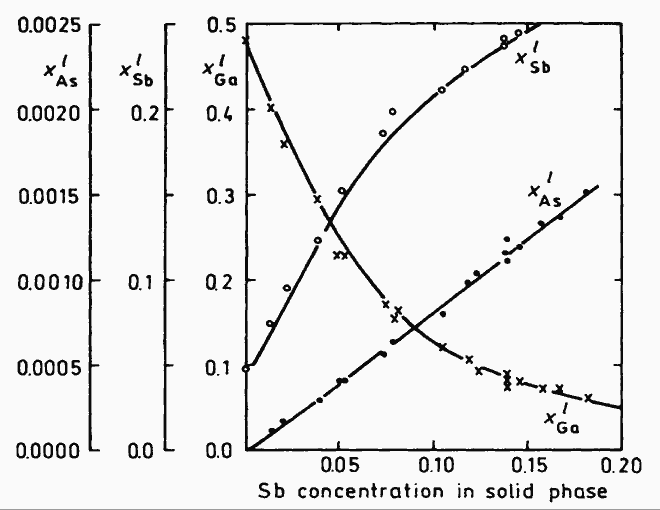
Key words crystal growth from melt — epitaxial growth — gallium compounds — III V semiconductors — indium antimonide — phase diagrams — semiconductor growth — phase diagram — liquid phase epitaxial growth — Ga sub x In sub 1 x Sb — liquidus data — In rich liqkide — DTA measurements — solidus data — regular solution ...
![Phase diagram of eutectic gallium-indium [5]. | Download ...](https://www.researchgate.net/publication/323553754/figure/fig3/AS:600806441091074@1520254826081/Temperature-coefficient-of-resistance-of-Ga-reproduced-from-19_Q320.jpg)
Phase diagram of eutectic gallium-indium [5]. | download ...
Gallium–indium nanoparticles as phase change material additives ...
![PDF] The phase diagram for the binary system indium-tellurium and ...](https://d3i71xaburhd42.cloudfront.net/24477405dc479b7ac9e4467376875671b2eb17bd/7-Figure3-1.png)
Pdf] the phase diagram for the binary system indium-tellurium and ...

Eutectic gallium-indium (egain): a liquid metal alloy for the ...

Bismuth–indium - wikipedia
Solved shown below is the gallium-indium phase diagram, | chegg.com
![PDF] Optical and Electrical Characterization of Melt-Grown Bulk ...](https://d3i71xaburhd42.cloudfront.net/64bb62af3b3d210d8d63e2a0c4449672fb26accc/25-Figure2.2-1.png)
Pdf] optical and electrical characterization of melt-grown bulk ...

Eutectic gallium-indium (egain): a liquid metal alloy for the ...

Study of the in–s phase diagram using spectrophotometric ...
Gallium–tin alloys as a low melting point liquid metal for ...

Metastable binary phase diagram of ga-in, reproduced from ref. [13 ...

Bismuth–indium - wikipedia
![Silver-indium phase diagram. [60] | Download Scientific Diagram](https://www.researchgate.net/profile/Ky-Cheong/publication/225404872/figure/fig3/AS:393642037530632@1470862983756/Silver-indium-phase-diagram-60.png)
Silver-indium phase diagram. [60] | download scientific diagram
Solved] the binary phase diagram for the gallium and indium system ...
![eutectic gallium-indium-tin phase diagram [6]. | Download ...](https://www.researchgate.net/publication/323553754/figure/fig2/AS:600806436909056@1520254825804/eutectic-gallium-indium-tin-phase-diagram-6.png)
Eutectic gallium-indium-tin phase diagram [6]. | download ...

Scielo - brasil - stability, mechanical properties and anisotropic ...
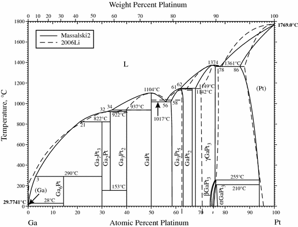
Ga-pt (gallium-platinum) | springerlink

Reprap: blog: a new approach to printing metals
0 Response to "37 gallium indium phase diagram"
Post a Comment