40 consider the circuit diagram depicted in the figure.
Consider the circuit diagram depicted in the figure. Now apply the loop rule to loop 1 the larger loop spanning the entire circuit. Assume that v 128 v r1 r2 r3 r4 r5 200 ω. B if the current through the top branch is i 2 0605 a. Consider a series rc circuit as in the figure below for which r 100 mω c 500 µf and ε 300 v. Answer to: Consider the circuit diagram depicted in the figure. a. What equation do you get when you apply the loop rule to the abcdefgha, in terms...
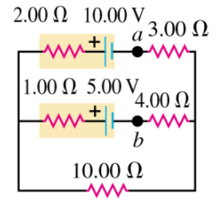
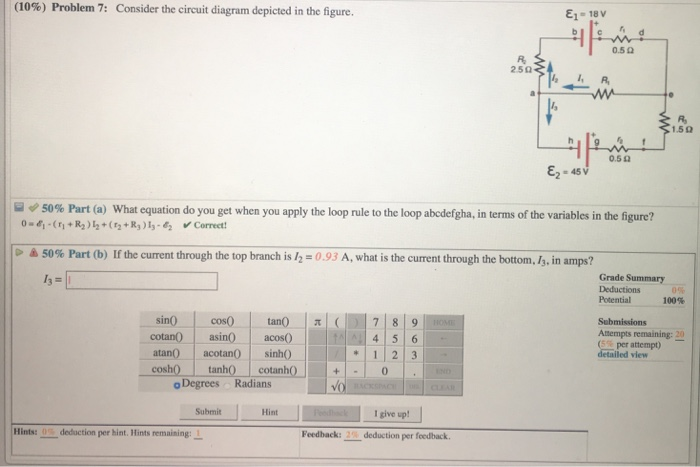
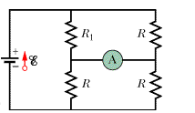
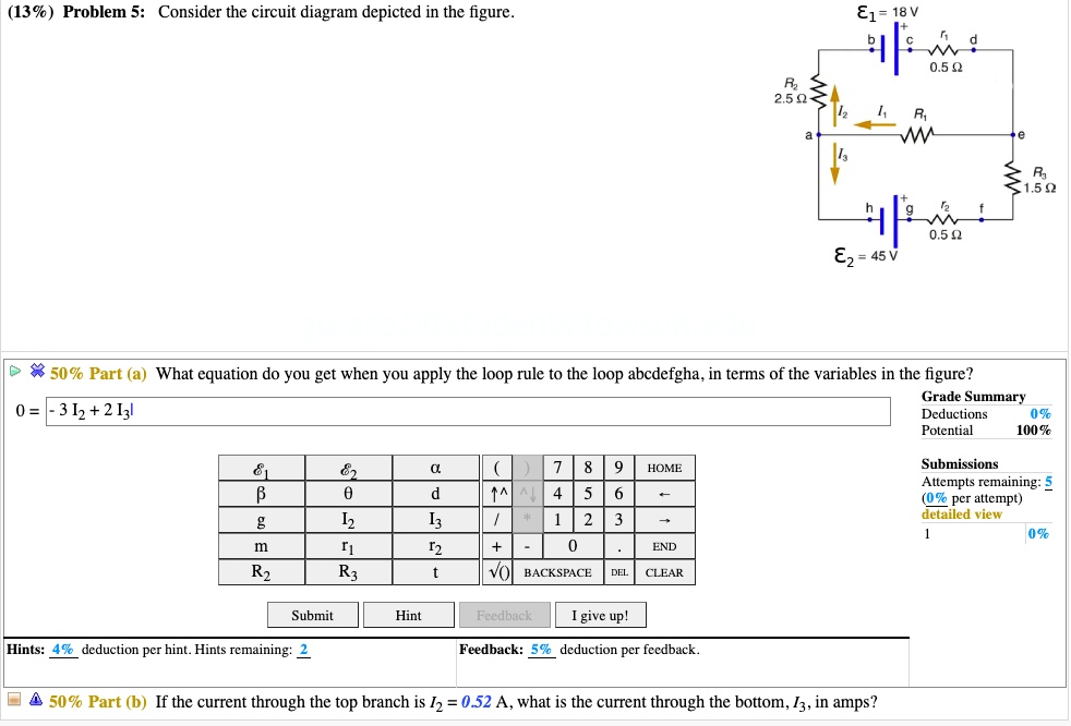
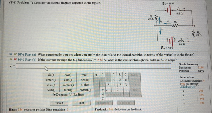
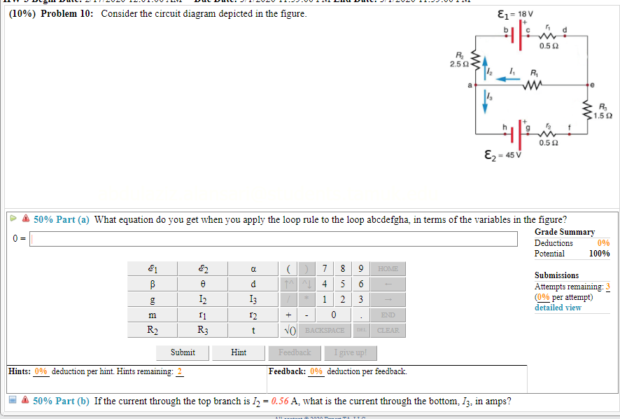
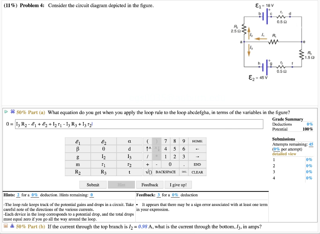
Question. Consider the circuit diagram depicted in the figure. What equation do you get when you apply the loop rule to the loop abcdefgha, in terms of the variables in the figure? 0 = If the current through the top branch is I_2 = 0.69 A, what is the current through the bottom, I_3, in amps?
Consider the circuit diagram depicted in the figure.
THE ASSIGNMENT: Consider the circuit depicted in the figure. By using the two following facts: (i) the voltage drop across a resistor is V = IR and (ii) the sum of all voltage drops in a closed loop sum to zero, The currents I1, I2, and I3 are determined from the 3 × 3 system. 91% (345 ratings) Problem Details. Consider the circuit diagram depicted in the figure. Part (a) What equation do you get when you apply the loop rule to the loop abcdefgha? Part (b) If the current through the top branch is I2 = 0.49 A, what is the current through the bottom I3, in amps? Frequently Asked Questions. 11/12/2019 · A transistor switch is a circuit in which the collector of the transistor is switched ON/OFF with relatively larger current in response to a correspondingly switching low current ON/OFF signal at its base emitter.. As an example, the following BJT configuration can be used as a switch for inverting an input signal for a computer logic circuit.
Consider the circuit diagram depicted in the figure.. Sample Circuit We consider the ... Consider the circuit shown in Figure P28.9. Find (a) the current in the 20.0-Ω resistor and (b) the ... Draw the circuit diagram and assign labels and symbols to all known and unknown quantities. Assign directions to the currents. Each electronic component in a given circuit will be depicted and in most cases its rating or other applicable component information will ... Figure 3 is an example of an electronic schematic diagram. Figure 3 Example of an Electronic Schematic Diagram ... Shown in Figure 4 is the schematic for a circuit and the Transcribed image text: (10%) Problem 5: Consider the circuit diagram depicted in the figure 0.5 Ω R2 2.5 Ω /2 R 1.5Ω 0.5 Ω 50% Part (a) what equation do you get when you apply the loop rule to the loop abcdergha, in terms of the variables in the figure? Grade= 100% Correct Answer Student Final Submission Feedback Correct! 012 R2+ 112 T3 R3 +32-62 0- 1-(Ti +R2) I2+(R3r2)13 2 Grade Summary ... %o ) Problem 4: Consider the circuit diagram depicted in the figure. E1= 18V 0.5 Q 25 0 1,5 0 0.5 4 82 45V 50 % Part (a) What equation do yOu get when YOu ...4 answers · Top answer: Yes. Question were given this circuit there. It's parts in this question. So in part A ...
The stick diagram for the CMOS N0R2 gate is shown in the figure given below; which corresponds directly to the layout, but does not contain W and L information. The diffusion areas are depicted by rectangles, the metal connections and solid lines and circles, respectively represent contacts, and the crosshatched strips represent the polysilicon ... Consider a series RC circuit as in the figure below for which R = 1.00 MΩ, C = 5.00 µF, and ε = 30.0 V. Find (a) the time constant of the circuit and (b) the... EECS 31/CSE 31/ICS 151 Homework 5 Questions with Solutions. View Questions Only View Questions with Strategies. Problem 1 Question (SR latch) Draw the output and timing diagram of a (a) NOR and (b) NAND implementation of an SR latch for the input signals depicted in Figure P6.2. Figure 6.13. State-assigned table for the sequential circuit in Figure 6.12. Present Next state state Outputs A 00 00 0 1 0 0 0 0 0 0 0 B 01 10 1 0 0 0 1 0 0 1 0 C 10 11 1 1 1 0 0 1 0 0 0 D 11 00 0 0 0 1 0 0 1 0 1
[Figure 1(b)]. The frequency-dependent chan-nel loss depicted in Figure 1(b) can be undone by means of a circuit having the inverse response, i.e., a high-pass filter (HPF). As illustrated in Figure 1(c), if subjected to such a response, the received data assumes its original, undispersed shape and more easily lends itself to detec-tion. In this problem, we will consider the following situation as depicted in the diagram: A block of mass m slides at a speed v along a horizontal smooth table. It next slides down a smooth ramp, descending a height h, and then slides along a horizontal rough floor, stopping eventually. Assume that the block slides slowly enough so that it Suppose that these systems are connected in series as depicted in Figure P3.10. Find the input-output relation for the overall interconnected system. Is this sys tem linear? Is it time-invariant? x[n] System 1 - System 2 System 3 y[n] Figure P3.10 (d) Consider a second series interconnection of the form of Figure P3.10 where the 7.1 Consider the timing diagram in Figure P7.1. Assuming that the D and Clock inputs shown are applied to the circuit in Figure 7.12, draw the waveforms for the Qa, Qb, Qc signals. 7.5 Given a 100-MHz clock signal, derive a circuit using D FF to generate 50-MHz and 25-MHz clock signals. Draw a timing diagram for all three clock signals, assuming
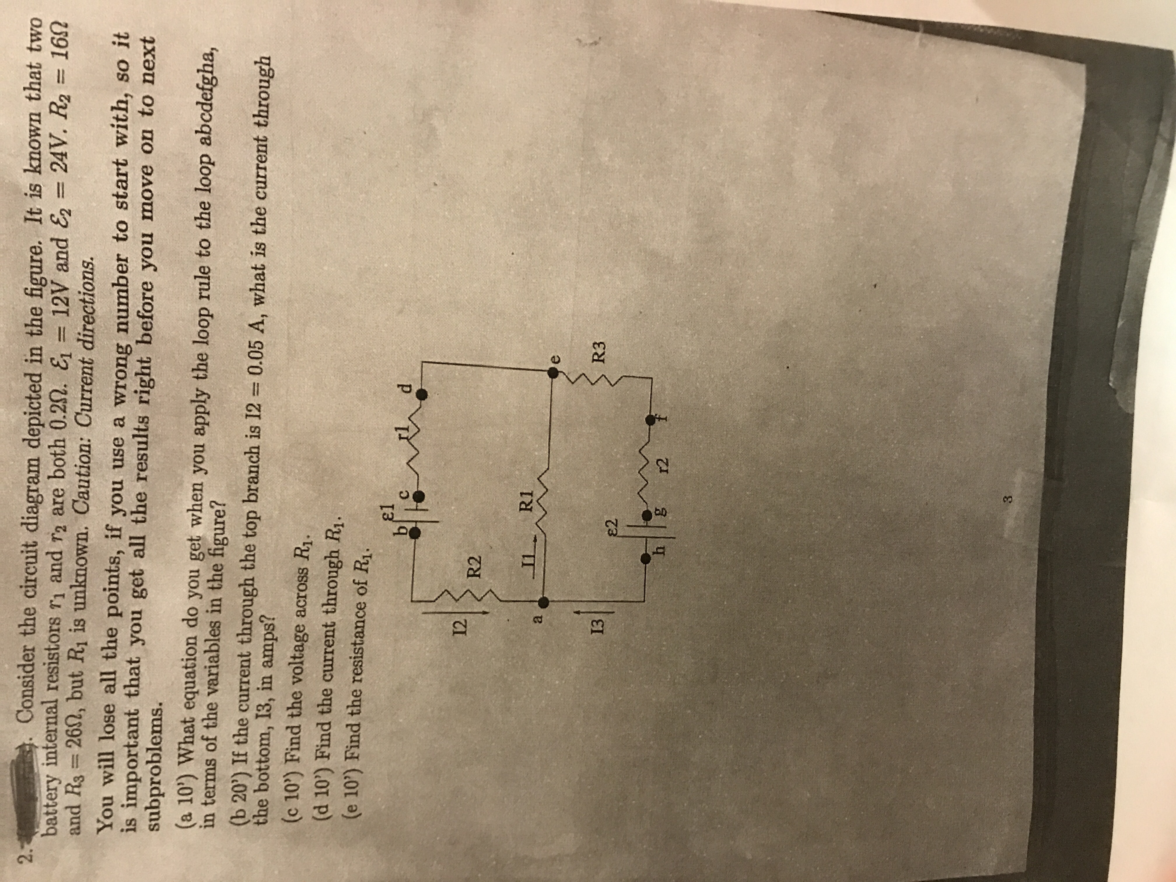
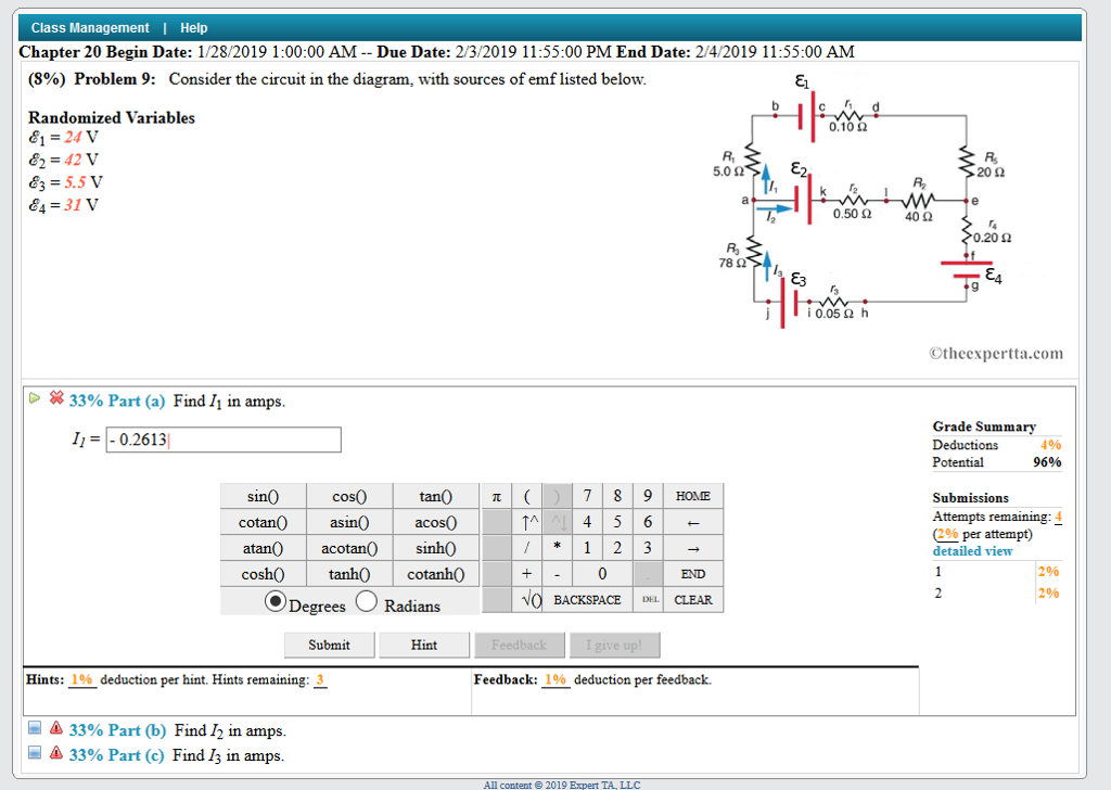
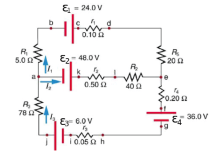
εί Consider the circuit diagram depicted in the figure. It is known that two 25Ω 24V and ε2 36V. R2 and R3-40f, but Ri is unknown. Caution: Current directions.

13/07/2019 · The circuit seen in the diagram above is a standard output current limiting protection circuit. Its operation is depicted in the diagram above: When the output current is too high, the voltage across RS (manganese copper wire) rises, and the voltage at pin 3 …
Determine the current in the 12-{eq}\Omega {/eq} resistor for the circuit shown in the figure assuming that the batteries are ideal. figure (a) 1.0 A ... Consider the circuit diagram depicted in ...
Jul 7, 2021 — Consider the circuit diagram depicted in the figure. {1= 18V 0. 52 2.523 om 3R 31.5.22 0.52 Ez = 45V What equation do you get when you apply ...
Consider the circuit that is to detect the sequence “1001” on a serial bit-stream data input and produce a logic 1 output when the sequence has been detected, as shown in Figure 5.72. The state machine will have three inputs—one Data_In to be monitored for the sequence and two control inputs, Clock and Reset—and one output, Detected.
P 5.2-2 Consider the circuit of Figure P 5.2-2. Find i a by simplifying the circuit (using source transformations) to a single-loop circuit so that you need to write only one KVL equation to find i a. Figure P 5.2-2 . Solution: Finally, apply KVL: 16 10 3 4 0 2.19 A aa 3 a

The equivalent circuit of this model is shown on Figure 9. R2 + + _ Vp Vn Vi Vo Ip In V in 1 I2 I1 R1 AVi Figure 9. Inverting amplifier circuit model Since our circuit is linear, the voltage at node 1 can be found by considering the principle of superposition. Vn is the sum of voltages Vn o and Vnin as shown on the circuits of Figure 10.

Consider the circuit shown in Figure (a). i L(0-) = 0, and v R(0-) = 0. But, -v R(0-) + v C(0-) + 10 = 0, or v C(0-) = -10V. (a) At t = 0+, since the inductor current and capacitor voltage cannot change abruptly, the ...
The corresponding electrical circuit is shown in the middle with the voltage and current traces depicted on the right. Current response in whole-cell configuration Looking at the current response to a voltage step, it is straightforward to pick apart which electrical properties contribute to …
Consider this diagram. Let us assume that it describes a series circuit containing a resistor, a capacitor, and an inductor. The current in the circuit has amplitude , as indicated in the figure. Which of the following choices gives the correct respective labels of the voltages across the resistor, the capacitor, and the inductor?
Transcribed image text: Consider the circuit diagram depicted in the figure. What equation do you get when you apply the loop rule to the loop abcdefgha, in terms of the variables in the figure? If the current through the top branch is I_2 = 0.47 A, what is the current through the bottom.

2. 27.3.2 (7, ex) Consider the circuit diagram depicted in the figure. (a) What equation do you get when you apply the loop rule to the loop abcdefgha, in terms of the variables in the figure? (b) If the current through the top branch is I2 = 0.085 A, what is the current through the bottom, I3, in amps? (c) Find the current through R 1 and the resistance of R 1.
Physics. Physics questions and answers. Consider the circuit diagram depicted in the figure. What equation do you get when you apply the loop rule to the loop abcdefgha? If the current through the top branch is I_2 = 0.49 A. what is the current through the bottom, I_3, in amps? Question: Consider the circuit diagram depicted in the figure.

For the action depicted in the figure, (Figure 2) indicate the direction of the induced current in the loop (clockwise, counterclockwise or zero, when seen from the right of the loop). The face of the south pole will become the north pole, so there will be a force of attraction between them, which makes the motion of the coil opposed.

Figure 12.2.2 (a) Time dependence of IR (t) and VR (t) across the resistor. (b) Phasor diagram for the resistive circuit. The behavior of IR (t)and can also be represented with a phasor diagram, as shown in Figure 12.2.2(b). A phasor is a rotating vector having the following properties: VR (t) (i) length: the length corresponds to the amplitude.

(b) The circuit diagram shows the shows battery as an emf source and an internal resistor. The two emf sources have identical emfs (each labeled by ) connected in parallel that produce the same emf. Consider the Kirchhoff analysis of the circuit in (Figure) (b).
06/02/2011 · Consider the instant, t = 0, when the switch in Figure 2.13 is closed. In order for any current to flow into the line, the source must see a finite impedance, which we now know to be the characteristic impedance of the line, Z o. It is worth remembering that, even though we are using the theoretical abstraction of an infinitely long line, which ...

View (3) Problem 30 Consider the circuit diagram in the figure. E1 = 18V.docx from AA 1 (3%) Problem 30: Consider the circuit diagram in the figure. E1 = 18V R Ez = 45 Otheexpertta.c 50% Part (a)
Answer to: For the circuit shown in the figure, V1 = 14.6 V and V2 = 9.4 V. Determine the current in the 4.0 ohm resistor. By signing up, you'll...
Consider the circuit diagram depicted in the figure. E1= 18V 2.5 9 8z 45 V What equation do you get when you apply the loop rule to the loop abcdefgha in ...5 answers · 6 votes: Show that Equation 32.28 in the text is Kirchhoff's loop rule as applied to the circuit in ...
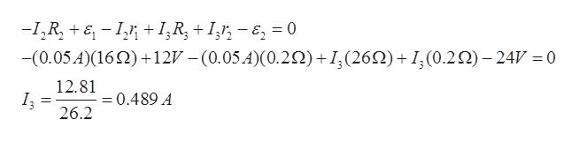
Figure 12.2.2 (a) Time dependence of IR (t) and VR (t) across the resistor. (b) Phasor diagram for the resistive circuit. The behavior of IR (t)and can also be represented with a phasor diagram, as shown in Figure 12.2.2(b). A phasor is a rotating vector having the following properties: VR (t) (i) length: the length corresponds to the amplitude.

Experiment with an electronics kit! Build circuits with batteries, resistors, ideal and non-Ohmic light bulbs, fuses, and switches. Determine if everyday objects are conductors or insulators, and take measurements with an ammeter and voltmeter. View the circuit as a schematic diagram, or switch to a lifelike view.

Consider the circuit diagram depicted in the fgure. It is known that two battery internal resistors r1and r2 are both 0.2Ω· = 12V and & = 24V. R2 16Ω 2. and Rs 262, but Ri is unknown. Caution: Current directions.
Question 1. (a) Consider the waveform below that has a period of T of 0.04 seconds. What is the rms voltage of this waveform? V(t) ...1 answer · 0 votes: Thorder to find the Thevenin equivalent impedance we have to Short Circuit all independent sources A (3-34). lon F ZAB - ZTH ZTH= 51 + [03-14). || ...

Consider the circuit diagram depicted in the figure. E- Ez. as v Part(a) What equation do you get when you apply the loop rule to the loop abedefgha, in terms of the variables in the figure? Expression : Select from the variables below to write your...
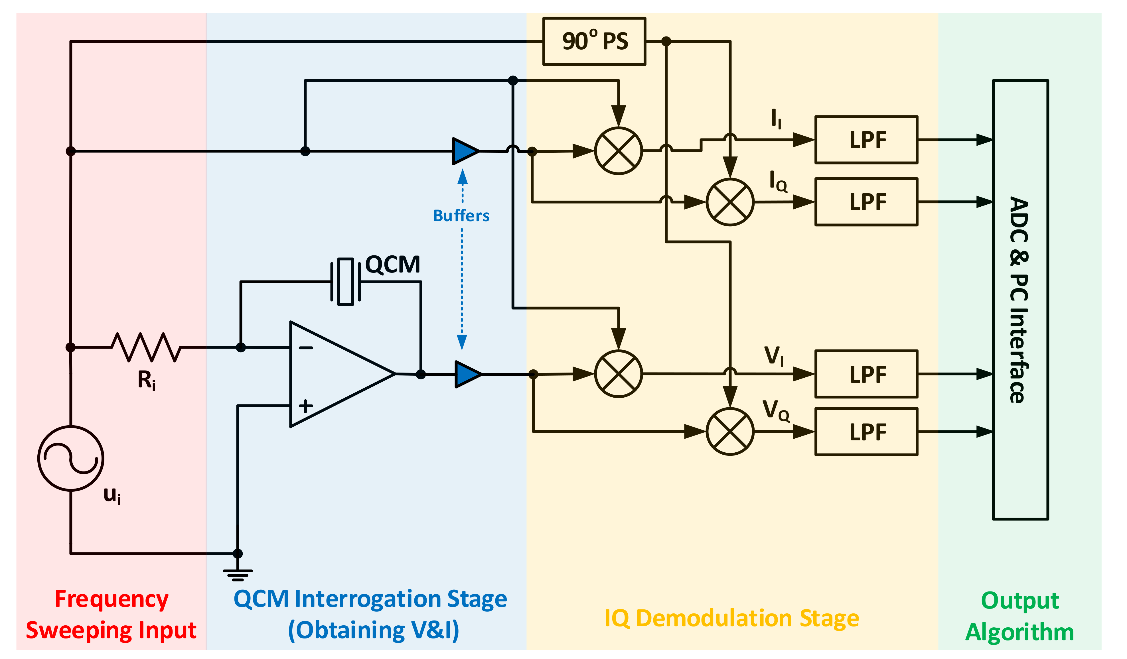
First we will consider the circuitry that amplifies and conditions the voltage to be measured (the “Amp” block in figure 1). The deflection of the oscilloscope beam is proportional to the input voltage (after ac or dc coupling). The amount of deflection (Volts/Division) depends upon the setting of the
11/12/2019 · A transistor switch is a circuit in which the collector of the transistor is switched ON/OFF with relatively larger current in response to a correspondingly switching low current ON/OFF signal at its base emitter.. As an example, the following BJT configuration can be used as a switch for inverting an input signal for a computer logic circuit.
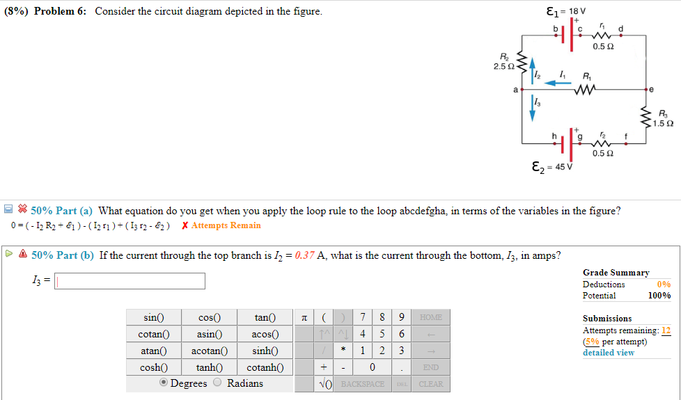
91% (345 ratings) Problem Details. Consider the circuit diagram depicted in the figure. Part (a) What equation do you get when you apply the loop rule to the loop abcdefgha? Part (b) If the current through the top branch is I2 = 0.49 A, what is the current through the bottom I3, in amps? Frequently Asked Questions.
THE ASSIGNMENT: Consider the circuit depicted in the figure. By using the two following facts: (i) the voltage drop across a resistor is V = IR and (ii) the sum of all voltage drops in a closed loop sum to zero, The currents I1, I2, and I3 are determined from the 3 × 3 system.


0 Response to "40 consider the circuit diagram depicted in the figure."
Post a Comment